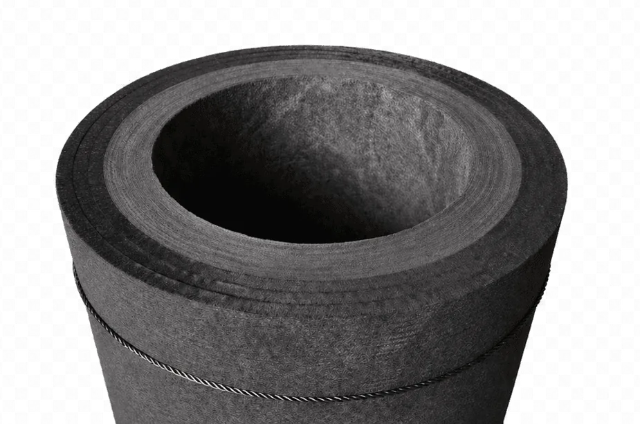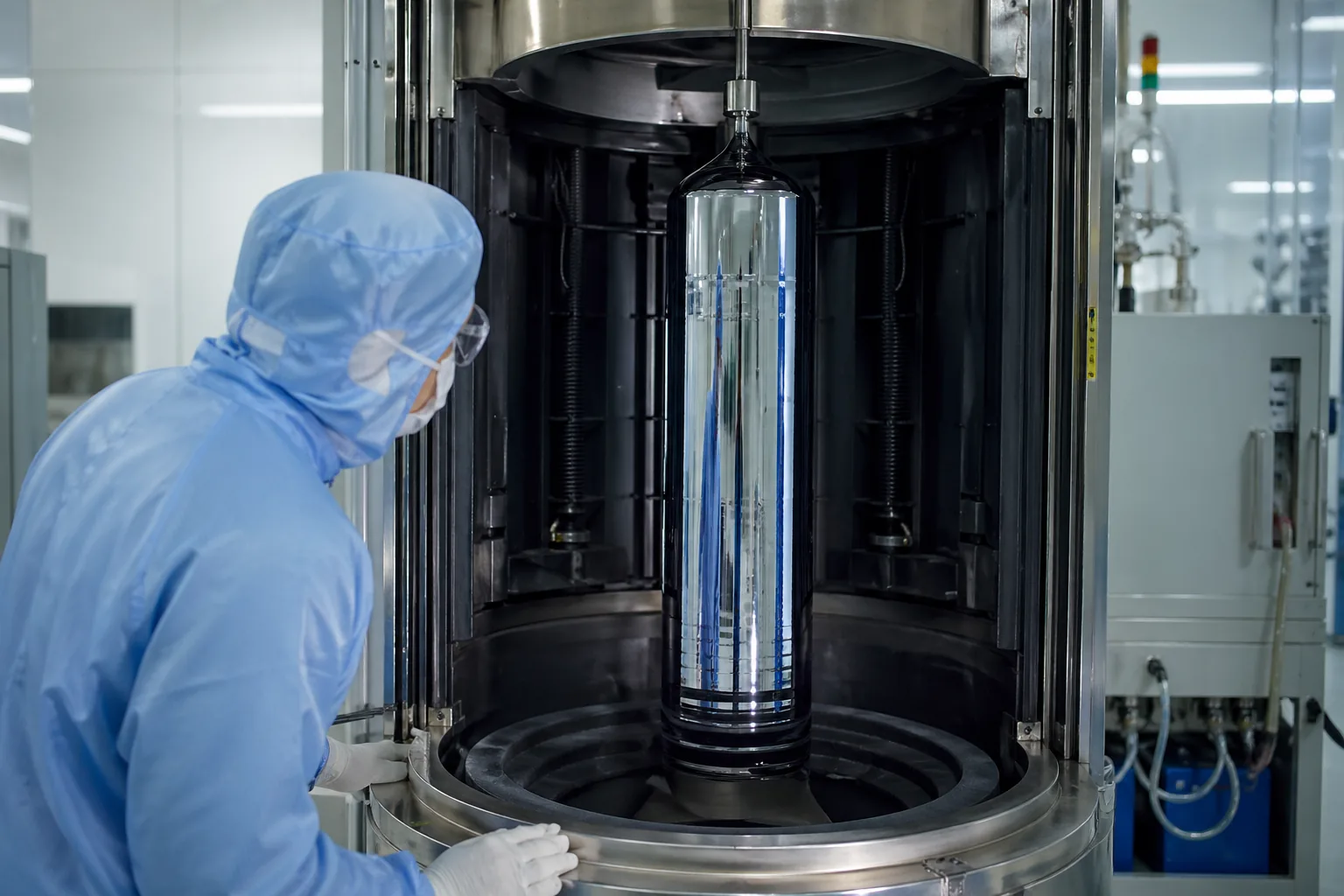
Every chip begins as a single crystal. From silicon Czochralski pulling to SiC physical vapor transport and the epitaxial layers that follow, critical steps take place inside hot zones running at 1,500°C to 2,200°C. At those temperatures, only a narrow set of materials remain stable. Carbon-based insulation helps control heat loss, chamber cleanliness, and long-cycle process stability.
Insulation defines the uniformity of the hot zone, the cleanliness of the growth chamber, and the long-term stability of the entire system. Customer requirements for thermal stability, purity, and conductivity shape every formulation we develop. The requirements show up in the details: a 12-inch silicon ingot held stable across a 120-hour cycle, or metallic contamination controlled at single-digit ppm levels under the corrosive vapor of SiC PVT.
AYD's role in the semiconductor value chain, illustrated with SiC PVT.
From powder synthesis through crystal growth to epitaxial deposition, AYD's high-purity carbon insulation supports three classes of core hot-zone furnaces: powder synthesis, crystal growth, and epitaxy. These furnace types operate continuously between 1,400°C and 2,200°C, where insulation purity, dimensional stability, and thermal conductivity must remain tightly controlled.
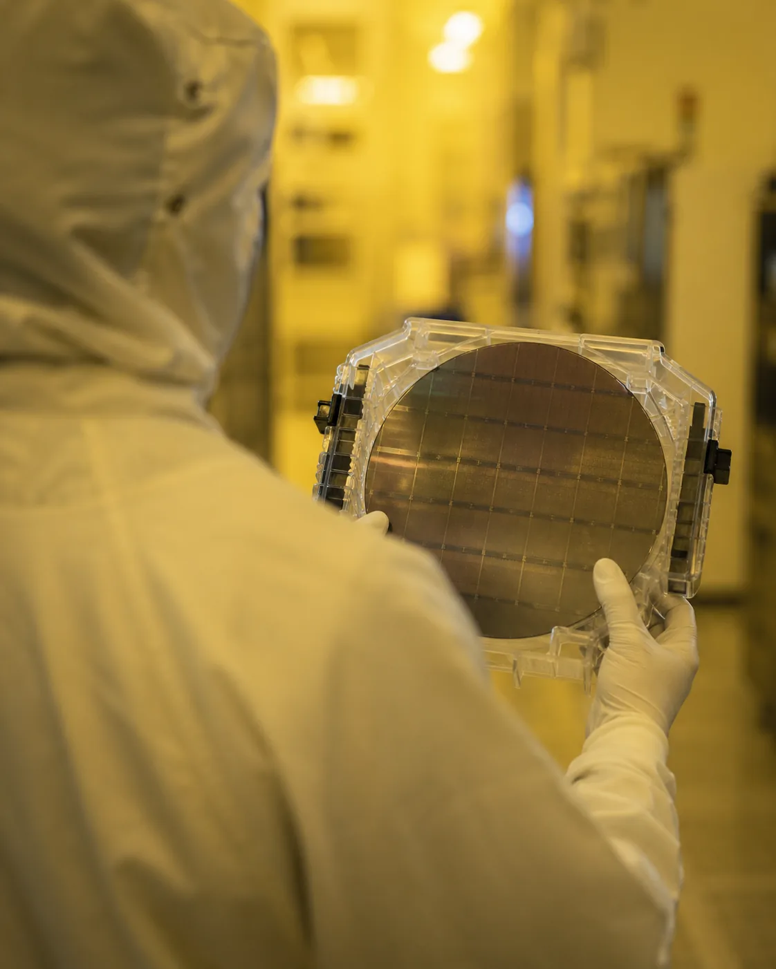
Semiconductor-grade purity verified by GDMS · density precision held across each production run · stable thermal conductivity at 2,000°C in vacuum · each component laser-etched and digitally traced.
Silicon Czochralski
Polycrystalline silicon is melted in a graphite crucible at 1,420°C, and a single crystal is pulled from the melt in the Czochralski (CZ) process. A 12-inch ingot can take 120 hours to grow.
Over such long cycles, the hot zone must remain highly stable. Even a small temperature drift can affect the full ingot, which is why customer standards for insulation are so demanding.
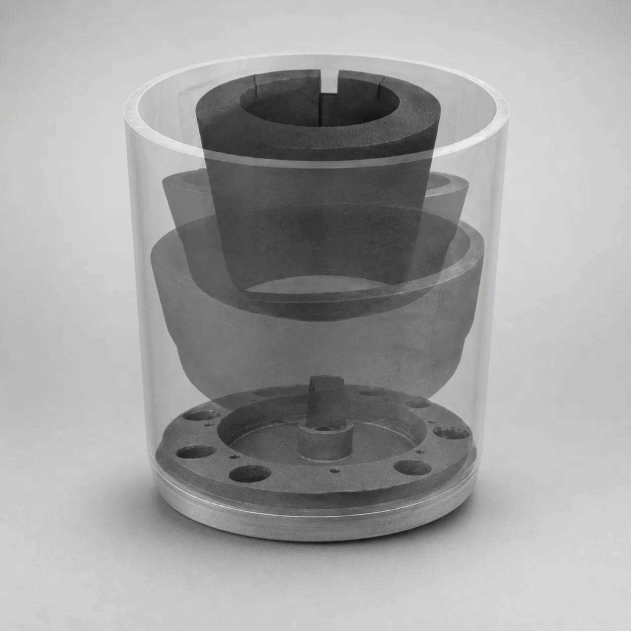
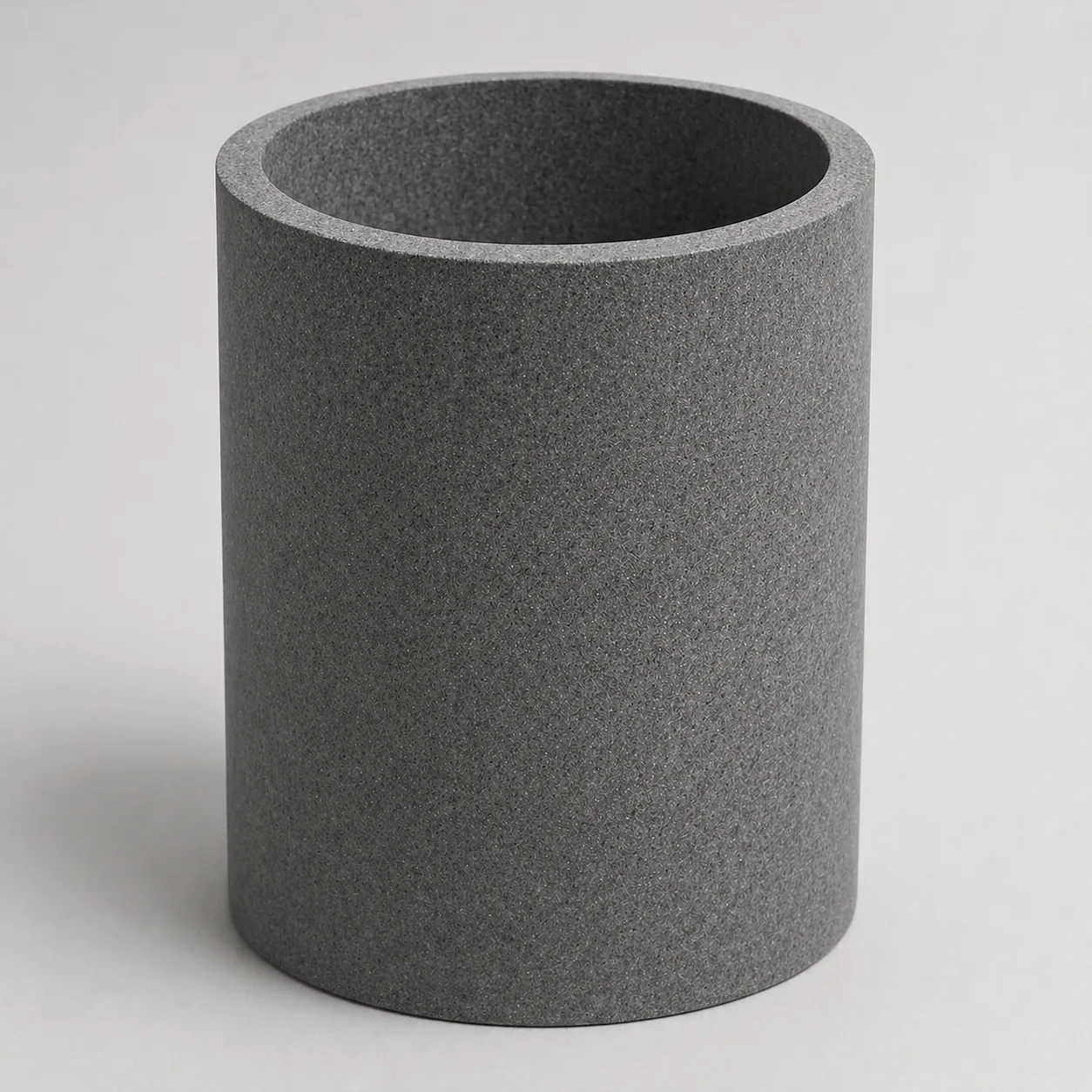
High-density rigid insulation forms the structural thermal envelope of the puller, combining mechanical strength for large-scale geometry with the high purity needed to keep metallic impurities away from the melt.
Silicon Carbide PVT
SiC does not melt; it sublimates. SiC powder is heated to 2,200°C and recondenses onto a seed crystal in a process called Physical Vapor Transport (PVT). It is a high-threshold crystal growth process used in advanced manufacturing.
High temperature combined with corrosive SiC vapor accelerates the breakdown of many materials. The materials that remain viable must meet a narrow set of requirements, making hot-zone engineering central to this process.
High-purity pitch-based soft felt remains chemically stable at 2,200°C. Ash content below 20 ppm helps reduce metallic vapor at the source. Precision-shaped rigid insulation supports axial gradient control inside the chamber.
Epitaxial Growth
On top of an existing wafer, a thin, low-defect single-crystal layer is grown via chemical vapor deposition (CVD), typically at 1,600–1,700°C for SiC epitaxy. This thin epitaxial layer is where power devices are built.
Temperature uniformity must reach ±2°C across the wafer surface, and the chamber must be free of volatile contaminants. Even trace organic residue can ruin the epitaxial layer.
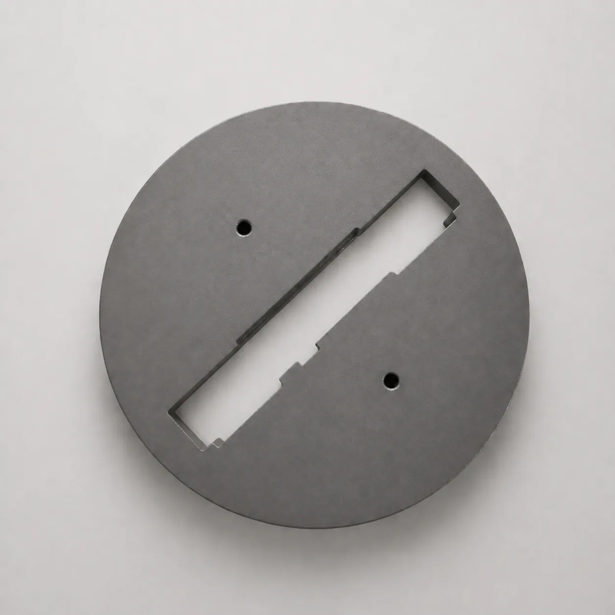
Purified-grade rigid and soft felt insulation forms the thermal envelope of the reactor, with low outgassing, uniform thermal conductivity, and stable corrosion resistance. AYD's Purified series (ash < 20 ppm, total metal impurities < 10 ppm) is engineered specifically for this class of application.
Rigid Insulation/Felt
Pitch- and Rayon-based rigid felt with precision machining and surface treatment options. Engineered for structural integrity in 12-inch CZ pullers and SiC PVT growth chambers.
View ProductSoft Felt
Rayon-based long-fiber needle-punched felt, high-purity, flexible wrapping for complex hot-zone geometries and corrosive vapor environments.
View ProductBuild your hot zone with us.
Share your hot-zone geometry, growth temperature, atmosphere, and purity target. AYD can recommend insulation materials, surface options, and qualification samples for SiC, GaN, and 12-inch silicon programs.